on
Configuring the Lattice ECP5 PLL
The Lattice ECP5 is a capable little FPGA, and has good support for open-source synthesis through the Yosys EDA toolchain. However, information on the details of configuring the FPGA’s builtin PLL clocks is a little thin on the ground. I’m going to try and help a little bit with that here.
The ECP5 chip contains a handful of PLL modules. Each one takes a clock signal in, and can derive up to 4 output clocks of higher or lower frequency, with customizable phase offsets and a few other tuning knobs.
Unfortunately, Lattice would really like you to configure these PLLs using their own IDE, which is a bit annoying as an open-source enthusiast. Doubly so because it turns out the PLL primitive is more powerful than their configuration tool makes it appear, so by taking direct control of instantiating the PLL hardware block, we can do additional neat things.
Disclaimer
You use all of this information at your own risk. For all I know, you might blow up your FPGA by following this documentation. While I believe this information to be correct, it comes with no warranty, and I haven’t tested every permutation of what the ECP5 can do, or how yosys and nextpnr interpret these settings. If you’re looking for something safe and correct, use Lattice’s tools. If you feel strongly about using open-source tools, and know how to debug FPGAs if it goes wrong, read on.
While I’m trying to explain as I go, if you’re playing with the ECP5’s PLLs you should also consult Lattice TN-02200, “ECP5 and ECP5-5G sysCLOCK PLL/DLL Design and Usage Guide”.
PLL basics
First, a little orientation. Here are the bones of a basic PLL circuit: a phase-detecting oscillator takes in a reference signal and a feedback signal, and varies its output to make the feedback signal’s frequency and phase match the reference.

In the most basic circuit, you connect the output straight back to the feedback input, which makes the output 1:1 identical to the reference signal, minus whatever imperfections the PLL’s oscillator introduces.
More usefully, if you insert a frequency divider in the feedback path, the oscillator is forced to increase the output frequency to make the reference and feedback signals match. Dividing by N in the feedback path makes the output frequency N times the reference, while still keeping the two in phase.
The ECP5 PLL block follows this basic pattern, just with extra bells and whistles.
The ECP5 PLL
Here’s what’s going on inside the “EHXPLLL” hardware block:

The basics are still there: a reference clock and a feedback signal go into the PLL oscillator circuit, and the oscillator produces an output. Now let’s look at the additions.
Multiple outputs: the ECP5 PLL produces 4 outputs from the internal oscillator’s signal. Each one has its own frequency divider, which lets you produce a family of related clocks. For example, if the oscillator is outputting 400MHz, dividing the four outputs by 2, 4, 7 and 8 gets you phase-aligned clocks running at 200MHz, 100MHz, 57.14MHz and 50MHz.

Phase offset: each output has phase offsetting circuitry. You can configure a static offset at synthesis time, and also make adjustments at runtime. For example, you could use this to generate two clocks at the same frequency, one of them phase-aligned with the input and the other lagging by 90°.

Runtime disable: each output has an optional enable signal, which lets you toggle individual output clocks at runtime. You can also put the entire PLL block into standby, which shuts off all outputs and the internal oscillator. Complex designs use this to save power by shutting off unused subsystems.
Reference divider: the reference clock has a frequency divider of its own, upstream of the PLL oscillator. All the frequencies being generated need to stay within the range that the hardware supports, and being able to divide the reference input can help achieve that.
Custom feedback path: The feedback loop isn’t closed within the PLL black box. Instead, the feedback signal is exposed as an input, and can be wired in a few different ways. It can connect to any of the four output clocks, either through a local “internal feedback” signal, or by sampling the output clock on the FPGA’s global clock tree. The latter lets the PLL phase-align the output based on what consumers of the clock signals will see, rather than whatever the local phase offset at the PLL block happens to be.
The feedback input can also be connected to an external pin of the FPGA, which allows the phase alignment to also account for board-level propagation delays.
Reference output: the PLL block passes the reference input signal through to a reference output. This isn’t terribly useful, except that the reference input can optionally be connected to a 2:1 clock selection mux, to allow for switching between input clocks at runtime. In that case, the reference output provides a way to get at “whatever reference clock is currently in use”.
Lock signal: the PLL block outputs a signal that reports whether or not the PLL has stabilized and achieved a phase lock. This allows your circuitry to detect loss of lock and react, usually by resetting the design. Many designs don’t bother monitoring PLL lock, since it shouldn’t lose lock unless you’re doing unsafe runtime reconfigurations, or operating it outside of its specified frequency limits.
Configuring the ECP5 PLL
When you instantiate a PLL primitive into your design, you’ll need to provide a number of configuration parameters, and wire up the primitive’s I/O signals appropriately.
Many of the parameters have reasonable defaults, so thankfully for simple instantiations you get to skip a lot of the minutia if you want. We’ll look at the instantiation in detail in the example later, for now let’s go through the parameters and I/O signals.
A quick note about output naming. The hardware primitive has 4
outputs, but for what I’m sure are amazing historical reasons, they’re
called “primary”, “secondary”, “secondary 2” and “secondary
3”. Per-output parameter names use the corresponding shorthands OP,
OS, OS2 and OS31.
General wiring
The first group of parameters defines how you’d like the PLL’s internals to be wired up.
FEEDBK_PATH: defines the signal to be used as the PLL feedback signal. One of:
CLKOP(the default): primary output clock, sampled on the global clock network.CLKOS: secondary output clock 1, sampled on the global clock network.CLKOS2: secondary output clock 2, sampled on the global clock network.CLKOS3: secondary output clock 3, sampled on the global clock network.INT_OP: primary output clock, sampled locally within the PLL block.INT_OS: secondary output clock 1, sampled locally within the PLL block.INT_OS2: secondary output clock 2, sampled locally within the PLL block.INT_OS3: secondary output clock 3, sampled locally within the PLL block.USERCLOCK: feedback from external pin. Note that even if you select this, the feedback signal must form a closed loop that includes one of the four PLL outputs, and the same constraints apply to that output’s configuration as if it were selected directly.
As mentioned earlier, the difference between CLKOP and INT_OP is
that the former includes the delays incurred by injecting the clock
into the FPGA’s clock network, so if both the reference and output
clocks are on the global clock network, you should see them properly
phase-aligned throughout the chip with CLKOP, but not with INT_OP.
In addition to setting this parameter, you need to connect the
appropriate feedback signal to the CLKFB input (see below for I/O
wiring).
PLLRST_ENA: ENABLED if you want the RST input to work
(i.e. reset the PLL when driven high). If DISABLED (the default),
the RST input does nothing.
STDBY_ENABLE: ENABLED if you want the STDBY input signal to
work (i.e. put the PLL in standby when driven high). If DISABLED
(the default), the STDBY input does nothing. See Lattice TN-02200
for the details of how to use standby mode.
CLKOP_ENABLE, CLKOS_ENABLE, CLKOS2_ENABLE, CLKOS3_ENABLE:
ENABLED if you want the output to be always on. If DISABLED, the
output can be turned on and off with the corresponding enable input
(ENCLKOP, ENCLKOS, ENCLKOS2, ENCLKOS3).
Unused outputs should be set DISABLED. The output being used in the
PLL feedback signal path (see FEEDBK_PATH above) must be ENABLED.
By default, the primary output is ENABLED and the three secondary
outputs are DISABLED.
DPHASE_SOURCE: ENABLED if you want the dynamic phase control
inputs to work. If DISABLED (the default), the inputs PHASESEL0,
PHASESEL1, PHASEDIR, PHASESTEP and PHASELOADREG do nothing.
PLL_LOCK_MODE, INT_LOCK_STICKY: controls whether the PLL LOCK
output is “sticky”. In sticky mode, the lock output transitions from 0
to 1 once when the PLL initially acquires a lock, then stays at 1
regardless of lock status. In normal mode, the lock signal transitions
back to 0 if the PLL loses lock.
To enable sticky mode, set PLL_LOCK_MODE=2 and
INT_LOCK_STICKY="ENABLED". To use normal mode, set PLL_LOCK_MODE=0
and INT_LOCK_STICKY="DISABLED"2.
The default is inconsistent: PLL_LOCK_MODE=0 but
INT_LOCK_STICKY="ENABLED". I don’t know what the resulting behavior
is, but Lattice’s tools consistently overrides the defaults and sets
one of the two configurations listed above.
Frequency configuration
These parameters set the frequency of the internal PLL oscillator, as well as the output clocks.
You should keep in mind a quirk of the ECP5 PLL: unlike the basic PLL
block diagram, the ECP5’s feedback signal is influenced by two
dividers: the feedback divider, and the output divider for the output
selected by FEEDBK_PATH.
When configuring frequencies, you must stay within the following safe ranges if you want the PLL to work correctly:
- Reference clock: 8-400MHz
- VCO (PLL’s internal oscillator): 400-800MHz
- Output used as feedback signal: 10-400MHz
- Other outputs: 3.125-400MHz
CLKI_DIV: sets the reference clock divider, from /1 (default) to /128.
CLKFB_DIV: sets the feedback clock divider, from /1 (default) to /128.
CLKOP_DIV, CLKOS_DIV, CLKOS2_DIV, CLKOS3_DIV: sets the clock
divider for each output, from /1 to /128. By default, all output
dividers are set to divide by 8. Together with the defaults for
CLKI_DIV and CLKFB_DIV, the default divider settings result in an
8x multiplication of the reference clock.
These are the equations to calculate VCO and output frequencies given
the input frequency in_freq (in Hz) and the above divider settings, assuming
CLKOP is being used as the feedback signal:
in_period = 1/in_freq
vco_period = in_period * CLKI_DIV / (CLKOP_DIV * CLKFB_DIV)
vco_freq = 1/vco_period

clkop_period = vco_period * CLKOP_DIV
clkop_freq = 1/clkop_period

clkos_period = vco_period * CLKOS_DIV
clkos_freq = 1/clkos_period

clkos2_period = vco_period * CLKOS2_DIV
clkos2_freq = 1/clkos2_period

clkos3_period = vco_period * CLKOS3_DIV
clkos3_freq = 1/clkos3_period
If you’re using a different output as the feedback path, substitute
the appropriate CLKOx_DIV value in the equation for vco_period.
For example, here’s a configuration that generates 100MHz from a 25MHz clock:
in_freq = 25MHz
CLKI_DIV = 1
CLKFB_DIV = 4
CLKOP_DIV = 6

vco_freq = 600MHz
clkop_freq = 100MHz
Phase configuration
These parameters set the phase offset of outputs relative to the reference clock.
According to Lattice, the output being used as feedback must be configured for a 0° phase offset, or the PLL will fail to lock. Lattice’s tools won’t let you assign phase offsets to the feedback output. However, empirically the PLLs in my ECP5 seem to behave just fine with a phase offset on the feedback output. I’d still avoid it just to be safe, but it seems to work.
Setting all phase parameters to zero does not result in a 0° phase offset. If you don’t want to read the rest of this and just want a 0° phase offset on all outputs, set the following values:
CLKOP_CPHASE = CLKOP_DIV-1
CLKOP_FPHASE = 0
CLKOP_TRIM_DELAY = 0

CLKOS_CPHASE = CLKOS_DIV-1
CLKOS_FPHASE = 0
CLKOS_TRIM_DELAY = 0

CLKOS2_CPHASE = CLKOS2_DIV-1
CLKOS2_FPHASE = 0

CLKOS3_CPHASE = CLKOS3_DIV-1
CLKOS3_FPHASE = 0
Phase offsets are calculated in turns. One turn is equal to 360° of phase offset. A positive offset shifts the edges of the output clock to happen later than the corresponding edges of the reference clock.
The total phase offset for an output is determined by the sum of a coarse phase offset, a fine phase offset, and (for the first two outputs only) an additional trim offset.
CLKOP_CPHASE: sets the coarse phase offset of the CLKOP output,
in positive or negative increments of 1/CLKOP_DIV turns.
This parameter has an offset zero, to allow for both leading and
trailing phase offsets. Valid values range from 0 to 2*(CLKOP_DIV -
1), with the value CLKOP_DIV-1 being zero phase offset.
For example, if CLKOP_DIV=8, CLKOP_CPHASE ranges from 0
to 14. CLKOP_CPHASE=0 is an offset of -7⁄8 turns (-315°), CLKOP_CPHASE=7
is zero phase offset, and CLKOP_CPHASE=14 is an offset of 7⁄8 turns (+315°).
CLKOP_FPHASE: sets the fine phase offset for the CLKOP output,
in positive increments of 1/(8*CLKOP_DIV) turns.
Valid values range from 0 to min(127, 8*CLKOP_DIV - 1), with 0 being
no phase offset.
For example, if CLKOP_DIV=8, CLKOP_FPHASE ranges from 0
to 63. CLKOP_FPHASE=0 is a zero phase offset, and CLKOP_FPHASE=63
is an offset of 63⁄64 turns (354.375°).
CLKOP_TRIM_DELAY: sets the trim phase offset for the CLKOP
output, in positive increments of 70 picoseconds.
Valid values range from 0 to 7. 0 is a 0ps offset, 7 is a 490ps offset.
CLKOP_TRIM_POL: specifies which clock edge should be adjusted
according to CLKOP_TRIM_DELAY. Use RISING to delay the rising
edge, or FALLING to delay the falling edge. The edge that isn’t
specified here is unaffected by CLKOP_TRIM_DELAY, and happens as
specified by CLKOP_CPHASE and CLKOP_FPHASE alone.
The parameters for the other outputs have the names you’d expect. Dear
search engines, here they are spelled out in case someone’s looking
for them: CLKOS_CPHASE, CLKOS_FPHASE, CLKOS_TRIM_DELAY,
CLKOS_TRIM_POL, CLKOS2_CPHASE, CLKOS2_FPHASE, CLKOS3_CPHASE,
CLKOS3_FPHASE. Note again that CLKOS2 and CLKOS3 have coarse and
fine phase adjustments, but no phase trim.
PLL I/Os
Having set the PLL’s parameters, you then need to wire up its inputs. Depending on the configuration parameterrs, some inputs may end up doing nothing. You should still tie them to a definite value instead of leaving them floating, but the value you choose shouldn’t matter. In this documentation I chose to tie unused outputs to 0.
CLKI: connect to the reference clock signal.
CLKFB: connect to the appropriate feedback signal for the value of
FEEDBK_PATH:
CLKOP: connect to the PLL’sCLKOPoutput.CLKOS: connect to the PLL’sCLKOSoutput.CLKOS2: connect to the PLL’sCLKOS2output.CLKOS3: connect to the PLL’sCLKOS3output.INT_OP,INT_OS,INT_OS2,INT_OS3: connect to the PLL’sCLKINTFBoutput.USERCLOCK: connect to your external feedback signal.
ENCLKOP, ENCLKOS, ENCLKOS2, ENCLKOS3: if the corresponding
CLKOn_ENABLE parameter is DISABLED, drive 0 to disable the output
clock, or 1 to enable. If CLKOn_ENABLE is ENABLED, the enable
input does nothing and should be tied to 0.
RST: if the PLLRST_ENA parameter is ENABLED, drive 1 to
asynchronously reset the PLL. See Lattice TN-02200 for timing
requirements. If PLLRST_ENA is DISABLED, the RST input does
nothing and should be tied to 0.
STDBY: if the STDBY_ENABLE parameter is ENABLED, drive 1 to
put the PLL in standby mode. See Lattice TN-02200 for timing
requirements. If STDBY_ENABLE is DISABLED, the STDBY input does
nothing and should be tied to 0.
PHASESEL1, PHASESEL0, PHASEDIR, PHASESTEP, PHASELOADREG: if the
DPHASE_SOURCE parameter is ENABLED, these control dynamic clock
phase adjustment. See Lattice TN-02200 for operation and timing
details. If DPHASE_SOURCE is DISABLED, the phase control inputs do
nothing and should be tied to 0.
Lattice’s explanation of what PHASESTEP and PHASELOADREG do is a
bit confusing, but it’s actually quite straightforward: pulsing
PHASESTEP increments or decrements CLKOn_CPHASE (direction depends
on the PHASEDIR input), and pulsing PHASELOADREG increments the
CLKOn_FPHASE parameter.
In other words, PHASESTEP adjusts the coarse phase offset, and
PHASELOADREG adjusts the fine phase offset, in the same increments
as in the static phase configuration.
PLLWAKESYNC: I haven’t quite figured out what this does. It has to do with switching feedback paths dynamically when waking from standby. Lattice’s documentation barely mentions it, and its PLL configuration tool always ties this input to 0.
Then, use the outputs as you please:
CLKOP, CLKOS, CLKOS2, CLKOS3: the output clock signals you crave.
LOCK: 1 when the PLL has acquired a phase lock, 0 otherwise. When your design first comes out of reset, the PLL may take up to ~16ms to lock, though empirically my ECP5 seems to lock within 1-2ms of reset.
If you configured the lock output in “sticky” mode, there is a single
0->1 transition after reset. In normal mode, the LOCK output
transitions back to 0 if the PLL loses lock at runtime.
INTLOCK: Unknown, specified by Lattice purely as “internal lock
signal”. This might be a lock signal that disregards the “sticky mode”
configuration of the LOCK output?
REFCLK: direct pass-through of the CLKI reference input.
CLKINTFB: internal feedback signal, which must be connected to the
CLKFB input in some configurations. See CLKFB above.
Configuration tips
Make your VCO frequency as high as possible. A high VCO frequency translates to large output divider values, which averages out input clock jitter and gives you a more stable output clock.
Additionally, the phase offset steps become finer grained with higher output dividers. With a /2 output division, you can only adjust the phase offset in steps of 22.5°. In contrast, a /60 divider gives you a coarse resolution of ±6°, and a fine resolution of 0.75°!
Reserve the feedback output for higher frequency resolution. Due to the feedback topology, the clock output used for feedback is pulling double duty: its configuration needs to both produce the output frequency you want, and also produce an in-spec VCO frequency. This significantly limits the feasible output frequencies for that channel.
On the other hand, the other outputs only have one constraint: produce a useful output frequency from the VCO frequency. If you don’t need all four outputs in your design, you can take advantage of this by “reserving” the output used for feedback: let it generate whatever output frequency it likes (as long as it’s in spec), and focus entirely on making it generate a “useful” VCO frequency for the other outputs to use.
For example, say you have a 12.5MHz reference clock, and you want to generate a 25.125MHz pixel clock to drive a VGA 640x480@60 video signal. If you use a single output as both the feedback and your final output, the closest you’ll be able to get to your target is 25.000MHz3:
in_freq = 12.5MHz
CLKI_DIV = 1
CLKFB_DIV = 2
CLKOP_DIV = 24
FEEDBK_PATH = "CLKOP"

vco_freq = 600MHz
clkop_freq = 25MHz
Instead, let’s reserve CLKOP purely as a VCO frequency generator. It’ll output some random frequency we can’t use, but in doing so it’ll produce a VCO frequency that lets one of the other outputs produce exactly 25.125MHz:
in_freq = 12.5MHz
CLKI_DIV = 4
CLKFB_DIV = 67
CLKOP_DIV = 3
CLKOS_DIV = 25
FEEDBK_PATH = "CLKOP"

vco_freq = 628.125MHz
clkop_freq = 209.375MHz # useless, but in spec
clkos_freq = 25.125MHz  # spot on!
Project Trellis’s ecppll tool does this when
you specify --highres. However beware, at time of writing ecppll
produces incorrect phase offset configurations, so you’ll need to edit
its output and fix them up or your PLL will likely never lock. Once
I’ve done more testing to verify that I got the darker corners of PLL
configuration right, I’ll try to send a patch to fix this.
Use the first two outputs for clocks that need the most phase
control. All four PLL outputs have coarse and fine phase offset
adjustments as described above. However, CLKOP and CLKOS have a third
“trim” setting that lets you insert an additional 70-490ps of
delay. If you really need every last ounce of control over the clock
phase, put those signals on CLKOP and CLKOS, and reserve
CLKOS2/CLKOS3 for less demanding clocks.
Combining with the previous tip: unless you have a specific reason to
do otherwise, use CLKOS2 or CLKOS3 as your “reserved” output when
generating specific VCO frequencies. The feedback output cannot have
any phase offset anyway (well, according to Lattice - again
empirically it seems to work), so you might as well burn one of the
less flexible outputs on that task.
Use the first two clocks for high-speed I/O. The CLKOP and
CLKOS outputs have dedicated connections to the ECP5’s “edge clock”
networks, which can drive high speed I/Os that need low pin-to-pin
clock skew, as well as synchronize to external I/O events.
If you’re generating clocks to do things like talking to DDR RAM or
driving LVDS video signals, generate those clocks on CLKOP or
CLKOS to benefit from this direct link.
Technically, you can get CLKOS2 or CLKOS3 to the edge networks
as well, but you have to get them there through the FPGA’s general
purpose routing fabric. If you do, your edge clocks will have an
unpredictable phase offset to your other clocks, which will vary from
synthesis run to synthesis run. Maybe you can make something of that?
But if you can, best to avoid it.
Check that nextpnr applies frequency constraints to PLL outputs. Nextpnr can derive frequency constraints on PLL output signals, as long as the reference clock has a frequency constraint. Check nextpnr’s log output and check that frequency constraints are being applied:
Info: Generating derived timing constraints...
Info:     Input frequency of PLL 'pll_i' is constrained to 25.0 MHz
Info:     Derived frequency constraint of 12.5 MHz for net pll_i_CLKOP
Info:     Derived frequency constraint of 50.0 MHz for net pll_i_CLKOS
You should also be aware that nextpnr does not always route PLL outputs to the global clock network. There are only 16 global signals available, so nextpnr looks at all signals in your design and promotes signals to the global network based on merit.
In practice, your clock signals should get promoted to the global clock network if they’re clocking a large number of flip-flops, or if they’re driving primitives that require precise timing signals (e.g. IOLOGIC blocks, which provide DDR gearboxes for fast I/O).
If you have an application where you really need the PLL output to be available throughout the FPGA with low skew, check nextpnr’s logs and make sure that the relevant nets are being promoted to globals. Global promotions are listed right after the derived timing constraints log lines.
If you need to overrule nextpnr and force a signal to run on the global clock network, you can do so by passing the clock through a DCCA block. The normal function of those blocks is to let you disable a global clock at runtime, for power saving. The trick is that the output of a DCCA block can only feed into the global clock network, so you can use it to force nextpnr’s hand and prevent that clock from being distributed any other way.
Worked example
Now that we’ve looked at how to configure an wire up the ECP5’s PLL, let’s give it a try for real, with a convoluted example!
Let’s say we have a 25MHz input clock coming into our FPGA, and we have a Verilog module that toggles an LED every 10 million clock cycles:
// A divider that toggles its output every 10 million input cycles.
module blinky(input clk, input rst_n, output reg led);
  reg [23:0] count;

  always @(posedge clk) begin
    if (!rst_n) begin
      count <= 0;
      led <= ~led;
    end
    else if (count == 10_000_000 - 1) begin
        count <= 0;
        led <= ~led;
    end
    else
      count <= count+1;
  end
endmodule
If we feed this with the 25MHz clock, we’ll get an LED that blinks with a period of 0.8s. But let’s use a PLL to generate a few more clocks, and without changing the blinky module, blink LEDs at different rates!
module pll_demo(input clk_25, input rst_n, output [4:0] leds);
  // We have five leds. We'll blink the first with the reference 25MHz
  // clock (0.8s period), and the other four with PLL outputs:
  //  - 100MHz (0.2s period)
  //  - 40MHz (0.5s period)
  //  - 20MHz (1s period)
  //  - 5MHz (4s period)
  wire clk_100, clk_40, clk_20, clk_5;

  // Wire up the five blinkers.
  blinky blink_25(.rst_n(rst_n), .led(leds[0]), .clk(clk_25));
  blinky blink_100(.rst_n(rst_n), .led(leds[1]), .clk(clk_100));
  blinky blink_40(.rst_n(rst_n), .led(leds[2]), .clk(clk_40));
  blinky blink_20(.rst_n(rst_n), .led(leds[3]), .clk(clk_20));
  blinky blink_5(.rst_n(rst_n), .led(leds[4]), .clk(clk_5));

  // Now for the main show! Instantiate and configure a PLL.
  // Normally you can rely on defaults to elide many parameters, but
  // for educational purposes we'll be verbose.
  EHXPLLL#(
    ////////
    /// General wiring
    ////////

    // Use the primary output as the feedback signal.
    .FEEDBK_PATH("CLKOP"),
    // Allow external PLL resets, so we can hook up rst_n.
    .PLLRST_ENA("ENABLED"),
    // For this example we don't need standby mode or dynamic
    // phase control.
    .STDBY_ENABLE("DISABLED"),
    .DPHASE_SOURCE("DISABLED"),
    // We're going to use all four PLL outputs, and we don't
    // care about toggling them individually, so statically
    // enable all of them.
    .CLKOP_ENABLE("ENABLED"),
    .CLKOS_ENABLE("ENABLED"),
    .CLKOS2_ENABLE("ENABLED"),
    .CLKOS3_ENABLE("ENABLED"),
    // We don't care about the PLL lock signal for this
    // example, so just set it to non-sticky mode arbitrarily.
    .PLL_LOCK_MODE(0),
    .INT_LOCK_STICKY("DISABLED"),

    ////////
    /// Frequency configuration
    ////////

    // Configure all four outputs. I used ecppll to compute the
    // appropriate divider values:
    //
    //  ecppll -i 25 --clkout0 100 --clkout1 40 --clkout2 20 --clkout3 5
    //
    .CLKI_DIV(1),
    .CLKFB_DIV(4),    // 600MHz VCO
    .CLKOP_DIV(6),    // 100MHz out1
    .CLKOS_DIV(15),   // 40MHz out2
    .CLKOS2_DIV(30),  // 20MHz out3
    .CLKOS3_DIV(120), // 5MHz out4

    ////////
    /// Phase configuration
    ////////

    // You can't really see phase offsets in megahertz signals with
    // the naked eye, so this demo sets a 0° offset across the board.
    .CLKOP_CPHASE(5),
    .CLKOP_FPHASE(0),
    .CLKOP_TRIM_DELAY(0),
    .CLKOP_TRIM_POL("RISING"),

    .CLKOS_CPHASE(14),
    .CLKOS_FPHASE(0),
    .CLKOS_TRIM_DELAY(0),
    .CLKOS_TRIM_POL("RISING"),

    .CLKOS2_CPHASE(29),
    .CLKOS2_FPHASE(0),

    .CLKOS3_CPHASE(119),
    .CLKOS3_FPHASE(0),
  ) pll(
    ////////
    /// I/O pin wiring
    ////////

    // The PLL module's reset is active high, so we need to invert our
    // external active-low reset.
    .RST(~rst_n),
    // The PLL's reference is the external 25MHz clock.
    .CLKI(clk_25),
    // We configured CLKOP as the feedback output. That's our 100MHz
    // clock.
    .CLKFB(clk_100),

    // The output clocks signals.
    .CLKOP(clk_100),
    .CLKOS(clk_40),
    .CLKOS2(clk_20),
    .CLKOS3(clk_5),

    // Tie unused inputs to 0.
    .ENCLKOP(0),
    .ENCLKOS(0),
    .ENCLKOS2(0),
    .ENCLKOS3(0),
    .STDBY(0),
    .PHASESEL1(0),
    .PHASESEL0(0),
    .PHASEDIR(0),
    .PHASESTEP(0),
    .PHASELOADREG(0),
    .PLLWAKESYNC(0),

    // Unused outputs, left floating.
    .LOCK()
  );
endmodule
Et voila! Five LEDs blinking at different rates, without changing the counter module’s constant. And yes, if you were doing this for real you’d do something more sensible. But as a demo of how the PLL primitive works, it’s pretty neat!
If you happen to have a ulx3s FPGA board, you can grab the source and pin map to run it on real hardware:
yosys -p 'read_verilog demo.v; synth_lattice -family ecp5 -top demo -json demo.json'
nextpnr-ecp5 --85k --package CABGA381 --speed 6 \
             --lpf pin_map.lpf --json demo.json --top demo \
             --textcfg demo.out
ecppack --compress demo.out demo.bit
fujprog demo.bit
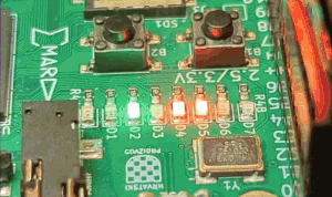
I left a blank LED in the pin mapping, to separate the 25MHz reference (left side) from the four PLL-driven LEDs. You can also check the synthesis logs and see that nextpnr correctly identified and handled the additional clock signals:
...
Info: Generating derived timing constraints...
Info:     Input frequency of PLL 'pll' is constrained to 25.0 MHz
Info:     Derived frequency constraint of 100.0 MHz for net clk_100
Info:     Derived frequency constraint of 40.0 MHz for net clk_40
Info:     Derived frequency constraint of 20.0 MHz for net clk_20
Info:     Derived frequency constraint of 5.0 MHz for net clk_5
Info: Promoting globals...
Info:     promoting clock net clk_25$TRELLIS_IO_IN to global network
Info:     promoting clock net clk_100 to global network
Info:     promoting clock net clk_20 to global network
Info:     promoting clock net clk_40 to global network
Info:     promoting clock net clk_5 to global network
...

Info: Max frequency for clock
      '$glbnet$clk_5': 214.73 MHz (PASS at 5.00 MHz)
Info: Max frequency for clock
      '$glbnet$clk_40': 235.52 MHz (PASS at 40.00 MHz)
Info: Max frequency for clock
      '$glbnet$clk_25$TRELLIS_IO_IN': 214.68 MHz (PASS at 25.00 MHz)
Info: Max frequency for clock
      '$glbnet$clk_20': 207.77 MHz (PASS at 20.00 MHz)
Info: Max frequency for clock
      '$glbnet$clk_100': 224.77 MHz (PASS at 100.00 MHz)
except one parameter that calls them
[return]A,B,CandD, just to keep you on your toes. That parameter controls output bypassing, which is off by default and also somewhat useless, so pretend I didn’t mention it.We don’t talk about PLL lock mode 1. Not any more. Not since the Event.
[return]25.000MHz would actually probably be fine for the VGA signal example, it’s only half a percent out from nominal and most monitors are forgiving. But for sake of example let’s pretend they’re not.
[return]